A game changer
for the photonics
industry
About
As the VCSEL sector is developing dynamically with lasers’ production expected to triple in the next five years, the project, with its innovative Ge-VCSEL solution, has the potential to be a game changer for the photonics industry. Demonstration of high performing devices of Ge-on-Si can unlock potentially large markets from optical data communications to imaging, lighting and displays, to the manufacturing sector, to life sciences, health care, security and safety. The new technology developed within the PhotoGeNIC project is expected to provide higher yields and severely reduced carbon footprint with recycling possibilities along every step. The projected results also include the production of larger Ge wafers with improved quality, uniformity and lower defects densities, which will enhance epitaxial technology on Ge substrates and increase the reliability of the device fabrication process.
Vision
The PhotoGeNIC consortium was born of the idea to introduce Ge substrates to the VCSELs manufacturing process. The goal is to meet the demand of constantly growing photonics market by providing a novel solution that will increase the production yield, reduce the defectivity, and introduce reduced impact on the environment. On top of that we believe that the project findings can be developed into usable tools and leave an innovative change across various end-user industries (e.g. e.g. automotive, smart phone, 3D sensing technologies)
Keyfacts
Reference
Reference Number:
101069490
Programme type:
Horizon Europe
Programme acronym:
HORIZON-CL4-2021-DIGITAL-EMERGING-01-07
Duration
Project Start:
01.10.2022
48 Months
Cost and Funding
Costs: € 4.788.752,00
Funding:
100,00% EU-funded
Motivation
The PhotoGeNIC team is driven by the desire to provide high performance and reliable laser technology to be integrated with leading edge CMOS technology as well as LiDARs. The consortium's ambition is to compare and demonstrate the advantages of the implementation of a novel VCSELs epi-structure grown on germanium (Ge) substrates instead of traditional gallium arsenide (GaAs). As Ge-based VCSEL is a new technology, we aim to focus on its non-toxic and infinitely recyclable feature to produce remarkable technology that will yield higher profit and decrease production losses.
Mission and Objectives
The proposal involves advanced photonics, and concerns semiconductor vertical-cavity surface-emitting lasers (VCSEL), widely used in the photonics industry, including short-distance communication systems, LIDARs, time-of-flight sensors, autonomous vehicles, robots and drones. Developing new VCSEL industrial technology with applied large diameter Ge substrates would bring novelty that has not yet been presented to the market. The main objectives of PhotoGeNIC project include:
• Mastering epitaxial growth technology of Ge-VCSEL structures and device fabrication
• Improving VCSEL’s spectral quality, optical power and reliability
• Lowering VCSELs’ environmental impact to meet the market growing requirements
• Integration with CMOS and miniaturization of technologies
Work Packages
WP1

Project, risk and innovation management
01.10.2022
30.09.2025
Detailed information
Assures operational, management and technical vitality of the PhotoGeNIC project encompassing management tasks on contractual, financial, legal, technical, administrative and ethical levels. The main objective is the establishment of a sound and flexible project management structure and an effective risk management strategy to avoid and react properly to deviations from the work plan.
WP2
Emerging technology for future VCSEL on Ge
01.10.2022
30.09.2025
Detailed information
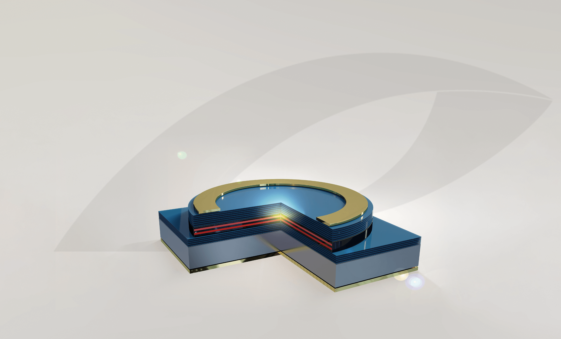
Aims at the development of the epitaxial growth of VCSEL structures on Ge substrates according to the proposed design. Ge is better lattice-matched to AlGaAs compounds building better VCSEL epi-stack than GaAs, which enables to significantly reduce residual strain, misfit defects and improve geometrical parameters as bow and warp. This makes it possible to overcome the limitations typical of GaAs and extend the wafer diameter to 200mm, which means higher yield and less production losses.
WP3

VCSEL/Ge processing and device characterization
01.10.2022
31.03.2025
Detailed information
Aims to achieve reliable fabrication process flow for VCSEL devices. The research will include different architecture configurations, optimization of technological process, creating better control and achieving higher reproducibility of Ge-based VCSELs.
WP4

New VCSEL functionalities and designs 1
01.10.2022
31.07.2025
Detailed information
Explores new functionalities and designs of VCSELs that are mainly focused on laser beam steering, and recently discovered Fano resonance as an efficient method for generation of stimulated light emission in sub micrometer size lasers. The aim is to control the optical beam emitted by developing additional external mechanical and optical systems.
WP5
Automotive LiDAR and industrial camera demonstrator
01.10.2022
30.09.2025
Detailed information
Aims to achieve seamless integration and performance of Ge-based VCSELs in a LiDAR demonstrator for automotive applications such as assisted driving functions, full autonomous driving as well as demonstrate improved characteristics of an industrial 3D camera in terms of image quality aspects.
WP6
Communication, Dissemination and Exploitation
01.10.2022
30.09.2025
Detailed information
Establishes a cross-project roadmap with clear communication, dissemination and exploitation activities. Communicates PhotoGeNIC progress and shares scientific results to create competitive advantages and handle all the Intellectual Property Rights achieved through the project.